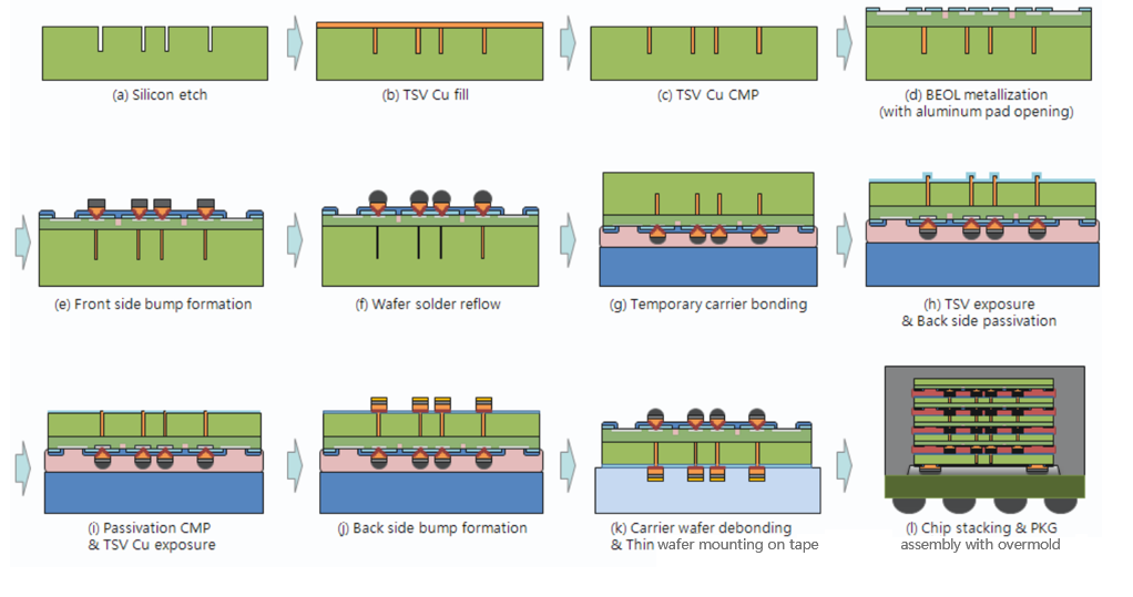
At present, the key to HBM manufacturing is TSV technology, which aims to drill holes on the chip. It is not a traditional wiring process like a lead frame, where pins (i.e. information entry points (I/O)) are pulled out and connected through wires. Drill a hole in the middle of the chip and fill it with a material that can transmit electrical signals well, such as copper (Cu). HBM has 1024 I/O numbers, which means TSV has 1024 holes drilled on the chip. This is a copper wire made of 1024 holes, each wire cleverly connected to another DRAM chip's wire, forming a long signal highway.
TSV technology provides a direct connection channel within the chip, minimizing the length of connections when connected to other chips. This can reduce resistance and accelerate data transmission speed. This process is the domain of the entire process executed within the wafer fab and is carried out in the following order:

-The methods for forming TSVs on silicon wafers include DRIE (deep reactive ion etching), metal assisted chemical etching, and the use of lasers. The commonly used methods for forming TSV include DRIE method and laser drilling method using Nd YAG. Due to the unevenness and roughness inside the through-hole, as well as the formation of silicon slag on the outer surface of the silicon wafer, the laser drilling method has limitations in application. DRIE technology is considered the most commonly used technique, used in approximately 95% of cases to form fine through holes.
1) Formation of through holes at the end of DRAM process:
-Etching is carried out during the process of hole formation, by depositing an insulating film at the etched site. Then fill copper into the TSV holes and polish them flat using CMP technology;
-After CMP grinding, the subsequent metallization process (BEOL, back-end metal routing process) begins;
-Solder bumps are formed on the front of the wafer;
Remove the bottom surface of the wafer to a certain thickness by grinding.
3) Chip cutting is generally completed using laser invisible cutting technology.
4) DRAM chips are stacked on top of buffer wafers.
5) CoWoS process
However, with the development of MR-MUF technology also transferring to HBM3 12 layer, a new technology (WSS technology) is needed to significantly reduce wafer warpage, while the wafer will continue to thin.
-WSS (Wafer Support System) is a process that uses carrier wafers to prevent wafer warping that occurs as the wafer becomes thinner.
Use temporary adhesive to connect the front side of the wafer with bumps to the carrier wafer, and then grind the back side to make the wafer thinner. Because it is attached to the carrier wafer, thinner wafers will not bend.
Use this structure to form protrusions on the back of thinner wafers. When bumps are formed on the front and back of the wafer, the core wafer is peeled off (carrier debonding), attached to a circular frame like in traditional packaging processes, and wafer cutting (sawing/cutting) is performed. The substrate is still attached to the carrier wafer, the chips cut from the core wafer are removed, and the chips are stacked on the substrate.
*Wafer bonding process
TC bonding is a "hot compression" method, in which after stacking DRAM chips and connecting them, the heated (hot) material is firmly pressed onto the top with a bucket (pressure compression). When bonding TC, a layer of "insulating film" called NCF is placed between DRAM chips. When the temperature exceeds a certain level, the film will melt and form connections between the bumps, fixing the two chips in place like a bonding agent and filling the space between the chips (known as bottom filling). It also acts as an insulator to control the current outside the bumps and wires. As is well known, NCF is a mixture of materials such as acrylic acid and epoxy resin, which is commonly used as an adhesive material. No matter how complex the machine bonding TC is, it is not easy to uniformly transfer the heat and pressure applied to the 1024 bumps on the chip. In addition to the 1024 wires used for transmitting electrical signals, there is also an auxiliary component called a "dummy bump" underneath the chip, which is used to absorb the heat generated everywhere. The increase of false bumps makes it difficult to evenly distribute physical energy throughout the entire area.
Before connecting the chip, the back of DRAM is usually ground to make it thinner and taller. If it is ground to an uneven thickness, the pressure on the chips will change again, resulting in a high defect rate. In addition, TC bonding is a process of applying pressure to each chip, so it is impossible to mass produce many chips at once.

This article is reprinted from the internet. If there is any infringement, please contact us to delete it. Thank you!

